Someone posted two circuit schematics side by side on r/electronics: a genuine Apple 5 W charger from roughly eighteen years ago, and a clone from the same era. Nearly four hundred upvotes and fifty-eight comments later, the interesting part is not the obvious headline.
The easy reading — genuine good, clone bad — falls short, and it is also unfair. What those two drawings actually show is an exact inventory of what gets deleted when a product is optimised for bill-of-materials cost. And nearly everything deleted turns out to be what the regulations require.
A note on the images: both schematics come from the original r/electronics thread posted by u/Dr-Double-A. The analysis and commentary in this article are ours.
Table of contents
The two schematics
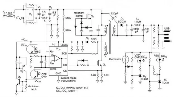
The first is the genuine charger. A flyback converter with a dedicated controller, input filtering, a snubber network, optocoupler feedback, a thermistor and several layers of protection.
The second is the clone. Same goal, same enclosure size, same connector, and roughly half the component count.
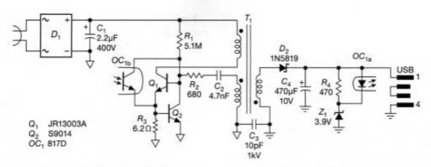
The difference in density is obvious at a glance. What matters, though, is what is missing, not how much.
What the genuine one has and the clone does not
The input filter
The genuine unit filters the mains input before rectifying. The clone goes straight in. That filter is not there for elegance: it is what stops the converter's switching noise — tens of thousands of times per second — from propagating through the building's wiring.
Without it, the charger becomes an emitter. That is exactly the failure that shows up in a conducted emissions test.
The Y capacitor
This is probably the most serious omission. The genuine design has a class-Y capacitor bridging primary and secondary, letting high-frequency noise find a return path without breaking the isolation between the hazardous side and the side you touch.
A Y capacitor is not an ordinary capacitor with a fancier name: it is certified to fail open. If it degrades, it stops conducting. An ordinary capacitor in that position can fail short, and then mains voltage appears directly on the USB connector.
This is where the jump happens. Removing the input filter degrades electromagnetic compatibility. Removing or downgrading the Y capacitor turns an EMC problem into an electrical safety problem.
The protections
The genuine charger carries overvoltage, overcurrent and over-temperature protection, plus a thermistor to limit inrush current. These are circuits that do nothing 99.9% of the time and exist purely for the remaining 0.1%.
Dedicated controller versus self-oscillator
The genuine unit uses a PWM controller with its control circuitry. The clone handles switching with a self-oscillator: a clever transistor arrangement that oscillates on its own, with no chip.
It works. In fact it works well while everything is fine. The difference lies in fault behaviour: a dedicated controller has soft start, cycle-by-cycle current limiting and a response decided by design. A self-oscillator responds according to circuit physics, which is not the same thing.
What the clone does get right
This is the part almost no article covers, and it came out in the thread from people who bothered to read the schematic rather than react to the headline.
- It senses voltage on the secondary. There are worse clones that sense on the primary and deliver an essentially unregulated output. This one closes the loop where the loop should be closed.
- It has some protection. The pair of transistors and a resistor that look like decoration actually act as an overload limit and, through thermal drift, as rudimentary temperature protection.
- There is an improvised snubber. Part of that same network damps switching spikes, assuming the winding is arranged the way it appears to be.
The honest conclusion is not that the clone is engineering-free nonsense. It is that it carries the minimum engineering needed to charge a phone, and not one component more. Everything removed was safety margin.
And to be fair to the era: genuine chargers from those years were not flawless either. Some units ran hot and there was a replacement programme. The difference is not that one was infallible — it is who answers when something goes wrong.
The bridge between D+ and D−
One detail in the clone's schematic confuses people seeing it for the first time: the two USB data lines are tied together.
It is not a mistake. It is the standard, cheapest way of telling the phone "this is a charger, not a computer port", so it permits itself to draw more current. The genuine design solves it more elaborately, with dividers encoding different available currents. Both are legitimate.
Why this is precisely a CE marking problem
Overlay the list of what the clone is missing onto the list of what European legislation requires, and they match almost part for part:
- The input filter and the Y capacitor are what electromagnetic compatibility testing measures.
- The isolation distances between primary and secondary, and the protections, are Low Voltage Directive territory.
- The documentation that would demonstrate any of it simply does not exist.
Which is why a product like this does not merely fail the tests: it was never designed to sit them. We go into it in our guide to CE marking costs and pre-compliance.
One myth worth dismantling along the way: it is widely repeated that a CE logo with the letters set close together means "China Export". No official marking by that name exists. What does exist are defined proportions for the logo, and many counterfeit products draw it badly — but that is a clue, not a regulatory category.
The design lesson
When someone asks us why a well-designed power supply costs more than seems reasonable, this pair of schematics answers better than any explanation.
The bill-of-materials difference between the two circuits is a few euros. The engineering difference is months. And the behavioural difference is invisible while everything works: it shows up the day there is a spike on the mains, a short in the cable, or simply moisture inside the enclosure.
It is the same logic we apply to PCB design and to electronic product development: the components removed to save money are usually the ones preventing the expensive failure. And if the product carries a battery, the conversation gets more complicated still, as we cover in CE marking for battery-powered products.
If you take one idea away: in power electronics, the components that visibly do nothing are precisely the ones you are paying for.
Frequently asked questions
Is a counterfeit charger always dangerous?
Not always, but the risk is not something the user can control. Two units of the same clone may carry different parts depending on the batch. With a reputable charger you buy a verified design and someone legally accountable; with a clone you buy a lottery you cannot inspect without destroying it.
What is a Y capacitor and why does it matter so much?
It is a safety capacitor bridging primary and secondary so high-frequency noise has a return path without compromising isolation. It is built to fail open, never short. Replacing it with an ordinary capacitor, or removing it, is exactly what turns an EMC problem into an electrical hazard.
Why does the clone tie the USB D+ and D- pins together?
It is the standard trick for dumb chargers. Shorting the two data lines tells the phone it is facing a charger rather than a computer port, so it allows itself to draw more current. It is not a defect: it is the cheap way to implement charger detection.
Is a self-oscillating circuit always worse than a PWM controller?
Not worse, blinder. A dedicated controller brings soft start, cycle-by-cycle current limiting, thermal protection and defined behaviour under fault. A self-oscillator works, and this one does work, but its response to an anomaly comes from circuit physics rather than a design decision.
What does this have to do with CE marking?
Everything. The input filter and the Y capacitor are precisely what electromagnetic compatibility testing measures. Isolation distances and protections are Low Voltage Directive territory. A product without those parts does not merely fail the tests: it was never designed to sit them.
Designing a product with power electronics?
We can review the design before it reaches the laboratory and tell you what will fail in testing, and why.